1. The $599 question
On 4 March 2026, Apple announced a $599 laptop. A week later it was on shelves. Three weeks after that, Asus’s co-CEO S.Y. Hsu was on his company’s Q4 2025 earnings call describing the MacBook Neo as “certainly a shock to the entire market.” His CFO Nick Wu, on the same call, conceded that Asus had been preparing for the launch since the second half of 2025, found the specs to have “some limitations,” and noted that Microsoft, Intel and AMD were now “seriously discussing” a response. By mid-April Apple had revised its 2026 production target from five to ten million units, told suppliers to chase, and was still quoting May delivery dates on its US store. Tim Cook called it Apple’s best launch week ever for first-time Mac customers.
In every major budget-laptop OEM, the people whose forecasts depend on the global sub-$700 market — a segment that ships roughly 40 to 60 million units a year, dominated by HP, Lenovo and Dell with razor-thin margins — spent the week doing arithmetic. They had just been smacked by a new vendor to the segment with a structurally lower cost basis than any of them could match. IDC slashed its 2026 PC shipment forecast three times in four months, from -2.4% in November 2025 to -11.3% in March 2026. Dell raised prices 15 to 20 per cent in mid-December. Asus has warned customers of 25 to 30 per cent price rises in Q2. The Neo did not cause this; the DRAM and NAND price spike caused most of it. The Neo is the product that arrives in the middle of it priced at $599, with 8GB of unified memory in the package, and untouched by either supply problem.
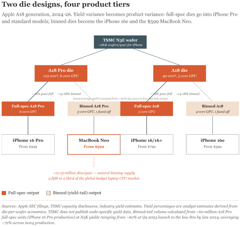
The problem Hsu and Wu were trying to parse on the earnings call boils down to the question “How is Apple selling that machine at that price?”. The answer is not engineering. The chip inside the Neo is the A18 Pro, the same silicon that shipped in the iPhone 16 Pro in September 2024 — but with one of its six GPU cores fused off. It is a binned part. The dies that come off TSMC’s N3E line for iPhone 16 Pro production sort, by yield variance, into two commercial bins: the full-spec part goes into a phone at $999; the one-core-defective part goes into a laptop at $599. The same wafer feeds both. The R&D was paid for by the iPhone Pro programme. The fab capacity was contracted by the iPhone Pro programme. The Neo gets the silicon at incremental cost approaching zero, because the silicon would otherwise be scrap.
This is not new behaviour. Apple has run the same pattern on the iPhone 16e (a binned A18, four GPU cores instead of five, $599) and is running it again on the iPhone 17e (binned A19) and the next generation of the Neo (rumoured binned A19 Pro). A four-tier product hierarchy financed by yield distribution. The binning mechanism explains the part of the cost advantage that no competitor can replicate. The missing OEM channel margin, the services-attachment economics, and a probably lower hardware margin than Apple’s Mac average explain the rest. It doesn’t need the hardware margin to match — it is making a fundamental play to alter the budget ecosystem in its direction. The rest is operational; the silicon is structural.
Hsu, asked to characterise the Neo on his earnings call, described it as a “content consumption” device, similar in his framing to an iPad rather than to a mainstream notebook. The collected press noted that Steve Ballmer said something similar about the iPhone in 2007.
The earnings-call question — how is Apple selling that machine at that price — does not have a satisfactory answer in the Asus competitive frame. Apple is not undercutting on margin. It is operating from a cost basis no vendor competing in the budget Windows segment can replicate. The mechanism is structural, has been visible in the silicon industry for a decade, and the MacBook Neo is the first product to make it legible at retail.
≈$0
The incremental cost of the silicon inside the MacBook Neo — a binned iPhone chip that would otherwise be scrap.
2. The flywheel
In semiconductor economics, the question that determines a product line’s cost basis is which other product line is paying for the process node. The R&D, the set-up costs, the wafer commitments: these are amortised against the highest-volume product on the node. Every other product on the same node gets the cost structure as inheritance.
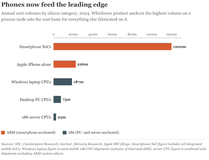
For TSMC’s N3E process — the second-generation 3-nanometre node that fabs the A18 and A18 Pro — the highest-volume product is the iPhone. Apple shipped about 226 million iPhones in 2024, of which the iPhone 16 family accounts for roughly 90 million, split across the A18 (90 mm² die) in the standard models and the A18 Pro (105 mm² die) in the Pro models. Working back from delivered units to wafer starts: at industry-estimated average N3E yields in the seventy per cent range, with conservative die-per-wafer counts at 300mm and Apple’s contractual structure of paying only for functional dies, the iPhone 16 production line consumes on the order of 180,000 N3E wafers per year. TSMC’s total N3-family capacity in 2024 ramped from roughly 70,000 wafers per month to 125,000 by year-end, an annualised average around 1.14 million wafers. iPhone 16 alone, or rather the A18 series of CPUs, is therefore consuming 15 to 20 per cent of TSMC’s leading-edge capacity. Add the M-series Mac CPUs for higher-end products and Apple’s share crosses 25 per cent.
No vendor outside the smartphone industry commits client-tier wafers at this scale on an advanced node. Intel manufactures most of its own consumer chips internally; AMD ships somewhere in the order of 30 to 40 million laptop CPUs a year on a mix of TSMC nodes; the entire Windows mobile CPU market is roughly 130 million units annually. None of these volumes are individually large enough to anchor a leading-edge node. The cost structure that Apple gets on N3E — the wafer-start commitment, the priority allocation, the yield learning curve already paid for — is unavailable to anyone else.
The yield curve does the rest. Even though TSMC does not publish node-specific yield data we can establish some figures from analyst estimates derived from die-per-wafer economics and supply-chain reporting. Industry sources suggest TSMC’s N3E yields ramping from approximately 60 per cent at Q4 2023 launch to the low 80s by late 2024, for an average of around 72%. Apple’s contract structure with TSMC is a “pay per good die” arrangement: TSMC absorbs unrecoverable yield as its own cost, prices yield risk into the functional-die rate, and Apple pays for working silicon. The economics are not that the wafers are free — Apple has paid for capacity allocation and process-node R&D through fifteen years of iPhone wafer commitments. The economics are that, having paid for the capacity, Apple has additional output available beyond the full-spec part. Of every hundred A18 Pro dies that come off the wafer, around seventy-two pass with all six GPU cores functional, and an estimated fourteen to eighteen are functional with one defective GPU core. The flawed-but-functional dies are an incremental revenue stream that Apple can monetise without further capital deployment. The MacBook Neo is the product that monetises them.
At iPhone 16 Pro production volumes — roughly 60 million units a year of full-spec A18 Pro — the binned tail at these estimated yield rates runs to 12 to 15 million dies a year. That is the natural supply of MacBook Neo silicon. It is also, by unit volume, somewhere between a fifth and a third of the entire global budget laptop CPU market. And that’s just the CPU. Apple piggy-backs on its mobile volume for NAND and memory as well — every component of the Neo’s bill of materials that scales with mobile volume inherits the same cost structure the silicon does.
The same dynamic explains x86’s own ascent in the 1990s. Intel’s Pentium server chips were not separately developed; they shared microarchitecture and process node with the desktop processor that was selling tens of millions of units a year into the consumer PC market. The PC volume paid for the node, the server got the cost structure. The mainframe and Unix workstation incumbents, building dedicated silicon at much smaller volumes, could not match the cost basis. By the late 1990s the question was not whether x86 would take the server market but how fast.
ARM is running the same play, one stack-level up. The smartphone is the new desktop PC. The laptop is the new server.
The standard engineering defense is that x86 does not actually have the architectural disadvantage the cost-structure argument implies. Modern x86 cores have not executed x86 instructions natively for twenty years; the decode stage translates the variable-length CISC stream into a sequence of fixed-width internal operations, and the execution engine that consumes those operations is, architecturally, a RISC core, not unlike ARM. This objection is correct, but not material. The decode frontend is not free: Intel’s optimisation manuals describe a µop cache of around 1,500 entries that exists specifically to avoid running the x86 decoder twice for the same instruction stream; AMD’s Zen equivalent is around 4,000. These caches are silicon spent on hiding the cost of the instruction set from the actual compute pipeline. Estimates of the decode-and-µop-cache share of die area on a modern high-performance x86 core range from five to fifteen per cent depending on configuration; the ARM equivalent is closer to zero. The translation layer that lets x86 keep its software compatibility costs silicon, on every die, on every node.
3. Who can run the flywheel
Apple is not the only vendor with phone-volume silicon. Qualcomm ships about 200 million Snapdragon SoCs into Android phones every year. MediaTek ships more again into the lower tiers of the same market. Rockchip and a long tail of Chinese SoC houses ship into industrial, embedded and white-label compute. The flywheel argument applies to all of them in principle. The question is which of them can actually run it.
Apple. The level of vertical integration achieved is the result of relentless business, product, and engineering rigour. The only step they outsource is the physical printing of the wafers — and even there, their lead-customer status treats TSMC as a de facto private foundry. Everything else is strictly in-house: the silicon design, the operating system, the developer toolchain, and the x86 translation layer. The Neo at $599 is the visible end of a vertical stack assembled deliberately over fifteen years for exactly this kind of move. The A18 Pro was designed for a phone, and the Neo carries the phone’s I/O constraints with it: two USB-C ports rather than four, only one of them USB-3, no Thunderbolt, Wi-Fi 6E rather than Wi-Fi 7. No other vendor in the budget laptop segment could ship those concessions at $599 and survive; Apple ships them and sells out for April. Rosetta 2, the binary-translation layer that runs x86 macOS applications on M-series silicon, is the most underestimated part of that stack. It runs at 70 to 80 per cent of native x86 performance — better than the architectural difference would predict — because Apple did something only a vertically-integrated vendor can do: the M-series cores have a special hardware mode for the strict memory consistency model x86 enforces, switchable at runtime. When Rosetta 2 is translating an x86 binary, the CPU itself enforces x86 memory semantics; the ARM weak memory model is only used for native ARM code. The performance cost of this mode is around nine per cent on average, avoiding the 40 to 60 per cent penalty that comes from software-emulating x86 memory ordering. Apple changed the silicon to make the translation efficient. No other vendor in the client compute market has all four of the properties that made this possible: silicon ownership, OS ownership, translator ownership, and the workload signal to know what to optimise the silicon for.
Qualcomm. Where the silicon works but the platform does not cooperate. Snapdragon X Elite, launched mid-2024, is by most independent benchmarks a competent laptop chip. It captured 0.8 per cent of the laptop market in Q3 2024 — about 720,000 units against a global notebook market of 66 million in that quarter. Qualcomm’s stated ambition for the segment was meaningfully higher than the result. The gap is the platform: Qualcomm sells silicon; Microsoft owns Windows; the OEMs own the channel. Microsoft’s Prism translation layer for Windows on ARM has had a slower and bumpier trajectory than Rosetta 2, for a structural reason: Microsoft has no incentive to break the x86 OEM ecosystem that ships most copies of Windows in the first place. The same vertical integration that lets Apple optimise silicon for its own translator pulls the other way for Microsoft. Qualcomm cannot fix this on its own. By late 2025 the company was visibly hedging, with Snapdragon X chips appearing in Android 16’s compatibility tables and a pivot toward Android laptops emerging as the public strategy. Hsu’s “content consumption” framing of the Neo, in this context, reads as the kind of thing said by a competitor whose own ARM laptop play has not worked.
MediaTek. The Taiwanese low-profile powerhouse that ships half a billion smartphone and embedded SoCs a year. MediaTek does not have a flagship Windows laptop, and does not appear to need one. It recently co-designed the GB10 chip in Nvidia’s $3,999 DGX Spark personal AI workstation: a 20-core ARM CPU paired with a Blackwell GPU on a coherent fabric. The architecture this points at is networking-up: build the access layer, build the developer relationships through embedded and IoT, partner with whoever owns the high-performance compute layer. MediaTek is positioning to be inside the next category of compute device the moment that category exists.
The Chinese SoC tier. Rockchip and Allwinner are not competing with Apple on performance. They are competing on cost and openness in industrial PCs, single-board computers, signage, automotive infotainment, and increasingly in sovereign-compute prototyping. Rockchip’s flagship parts use ARM Cortex-A application cores, where the Linux software ecosystem still wins. But every successive generation has added more RISC-V silicon as auxiliary or accelerator content. Their recent RV1106 already shipped with an ARM Cortex-A7 main core paired with a RISC-V MCU on-die. The RK182X coprocessor, announced in July 2025, is a multi-core RISC-V chip dedicated to running 3-billion- and 7-billion-parameter large language models locally. RISC-V is being used wherever the workload is constrained enough that the software ecosystem question doesn’t dominate, and the cost of adding it is an architectural licence fee Rockchip does not have to pay. Allwinner has gone further: its D1 series, in production since 2021, was the world’s first general-purpose system-on-chip built on T-Head’s open-source XuanTie RISC-V core, and ships into industrial, IoT and intelligent-voice products in volume alongside its ARM-based tablet line. The Chinese open-tier SoC vendors are running an architectural transition, in commercial product, that the policy actors in section 6 are still organising around.
4. The cloud and AI version
The same logic operates one stack-level up. Here, hyperscalers use cloud compute as their volume engine, driven by the need to escape external supplier roadmaps entirely.
Amazon’s AWS arrived at this conclusion long ago. Graviton 1 shipped in 2018 as a proof of concept that ARM silicon could host real compute workloads — meaning the design work was underway by 2016, the strategic decision earlier still. Graviton 4, generally available since July 2024, is the fourth generation: a 96-core Neoverse-V2 part now deployed across the AWS estate. AWS does not normally publish unit numbers for its silicon programme, but it has published two figures that are sufficient for the structural argument. At re:Invent 2024, vice-president Dave Brown disclosed that more than half of new EC2 vCPU capacity added across the prior two years had been Graviton rather than x86. By Q4 2025, on the parent company’s earnings call, Amazon reported that most new compute capacity was Graviton, that ninety per cent of AWS’s top thousand customers had Graviton in production, and that the chips business — Graviton plus the Trainium AI accelerator family — was now exceeding ten billion dollars in annualised run rate, growing at triple-digit rates year over year.
$10bn+
Annualised run rate of AWS’s chips business — Graviton plus Trainium — by Q4 2025, growing at triple-digit rates year over year.
The economics are the flywheel applied to instance volume rather than handset volume. EC2 sells at a price set by competition with Azure and GCP. Owning the silicon design rather than paying Intel or AMD’s gross margin on every chip — on top of the power saving the ARM architecture delivers — lowers the cost basis of every instance AWS sells, and the savings fund the next Graviton generation. AWS does not need to win the merchant CPU market; it needs to lower the cost of EC2.
Nvidia arrived at the same architectural answer through a different door. Nvidia is a GPU company, not a CPU company. Its problem with Intel and AMD’s server CPUs was structural, not commercial. Conventional server architecture connects CPU and GPU over PCIe, a bus designed for general expansion-card I/O — not for the streaming-throughput coherent-memory traffic AI training and inference workloads generate between the two. Xeon and EPYC fit the conventional model and inherit its bottleneck. Nvidia’s Grace CPU, announced 2022 and shipping in volume in the Grace Hopper Superchip, is an ARM-based design with a 900GB/s link to a Hopper or Blackwell GPU on the same package, replacing the PCIe bus with a memory-bandwidth-class interconnect that treats CPU and GPU as a single coherent compute system. The next-generation Vera CPU takes the logical step: Nvidia is now designing custom ARM-compatible cores under its own microarchitecture programme — Olympus — rather than licensing Neoverse off the shelf.
Nvidia is also already preparing for the architecture that comes after ARM. In July 2025, at the RISC-V Summit China in Shanghai, Nvidia’s vice-president of hardware engineering Frans Sijstermans announced that Nvidia is porting CUDA to RISC-V — meaning RISC-V CPUs will be supported as host application processors in CUDA-based AI systems, alongside x86 and ARM. The port targets the RVA23 RISC-V profile ratified in 2024. Nvidia framed the announcement as a “strategic technology disclosure” rather than a product launch, and has not committed to a release timeline. In a subsequent interview with RISC-V International, Sijstermans framed the rationale as structural: “as export controls and market fragmentation reshape the compute landscape, it’s increasingly important for foundational technologies like CUDA to be able to operate independently of any one architecture or licensing regime.”
The world’s dominant GPU company has concluded that the right CPU for AI infrastructure is one that is currently ARM, will be one Nvidia designs itself, and may eventually run on whatever architecture its customers can lawfully and affordably build.
The DGX Spark, launched late 2025 at $3,999, closes the loop visually: a 20-core ARM CPU (the GB10, co-designed with MediaTek), a Blackwell GPU, 128 gigabytes of unified memory, all in a 170-watt desktop enclosure that delivers personal-AI-workstation performance. ARM at the consumer edge in the MacBook Neo, ARM in the cloud at AWS, ARM in the AI training tier at Nvidia, ARM in the personal-AI tier at the Spark — and in every case, the ARM choice is provisional rather than terminal. Four different actors, four different forcing functions, the same silicon answer — for now.
AWS did not coordinate with the European Union’s chip-sovereignty programme. Nvidia did not consult India’s semiconductor policy. Apple did not synchronise its Mac transition with China’s RISC-V investment. Each of these actors solved its own dependency problem on its own terms; each ended up at custom ARM silicon; each is now quietly hedging the next architectural transition before the current one is complete. The convergence is not a fashion. It is what happens when the mechanism described in section 2 — high primary volume amortising the node, adjacent products inheriting the cost structure — is applied at every layer of the compute stack by actors with the resources to act on it.
The hyperscaler version of the flywheel got there first because the hyperscalers had the capital. The sovereign-compute version arrives next, with five years’ lag, with policy instead of capital, and with the architectural answer the consumer-tier and hyperscaler-tier actors are quietly already preparing for.
5. The incumbent trap
The structural argument so far implies that Intel and AMD should be the most alarmed companies in the sector. They are not. Their public statements through 2024 and 2025 have ranged from confident to defensive to dismissive. The incumbents’ calm surface is not strategic confidence; it is the predictable output of an incentive structure that makes accurate perception expensive.
Three forces operate on Intel and AMD simultaneously, and each pulls in the same direction.
The first is margin dependency. Intel’s Xeon and AMD’s EPYC server margins are the cash cows that fund the engineering programmes those companies need to compete on the next process node. Migrating away from x86 in any meaningful fraction of those product lines reduces the margin pool that pays for migrating away from x86. The capital-allocation logic does not work backwards from the long-run architectural conclusion; it works forwards from the next quarter’s free cash flow. Intel cannot fund a credible non-x86 server programme by cannibalising the x86 server programme that pays for it.
The second is customer dependency. The immense x86 installed base — every enterprise data centre running existing workloads on Xeon, every Windows OEM shipping consumer laptops, every government procurement contract specifying x86 compatibility, every line of legacy ERP code that nobody has the appetite to recompile — is the customer set whose continued purchasing keeps Intel and AMD solvent. That customer set wants x86 compatibility maintained, not abandoned. Each year Intel maintains backward compatibility is a year ARM gains ground without facing a structural response. Each time Intel announces a structural response is a time the installed base flinches.
The third is the architectural admission problem. If Intel publicly concedes that ARM is structurally more efficient for the workloads its customers care about, it accelerates the migration it is trying to slow. If it concedes nothing, it cannot redirect engineering effort toward the problem it actually faces. The policy that is least costly to communicate is “x86 is fine”; the policy that is most costly to communicate is the one most likely to be true. Intel is therefore stuck communicating the policy that is least costly, which is also the one that most prevents it from acting.
Intel’s renewed interest in the foundry side of its business is at least partly explained by this.
The trap closed over an eighteen-month window. In May 2023, Intel published the draft specification for x86-S, a simplification proposal that would have removed virtually all legacy design elements — paring x86 down to the actually-used sixty-four-bit subset. The proposal was an architectural admission in everything but name: it acknowledged that the legacy frontend was overhead worth removing. In June 2024 Intel published a revision 1.2. In December 2024, Intel terminated the x86-S programme. The official statement cited “inputs from the ecosystem” and reaffirmed Intel’s “longstanding commitment to software compatibility.” A new x86 Ecosystem Advisory Group was formed with AMD and the major Windows OEMs as members. In September 2025, AMD publicly stated that the ARM ISA does not offer an efficiency advantage over x86. Across eighteen months, Intel had drafted a simplification, attempted to ship it, been pushed back by the ecosystem it depended on, killed the programme, joined a defensive coalition with its main competitor, and watched that competitor publicly deny the architectural premise the simplification had implicitly accepted.
This is the trap closing. It is not that Intel and AMD do not understand what is happening to them. It is that the institutional cost of acting on that understanding is, at every decision point, higher than the cost of not acting. The customer base, the margin structure, and the public communication strategy are all locally optimised, and the local optima compose into a global outcome in which the incumbents are the last actors in the industry to be free to do what the structural argument requires.
One specific path remains for Intel that the structural argument does not foreclose. Intel 18A and the foundry pivot are a different bet entirely: rather than defending x86 as an architecture, become the merchant fab any architecture can use. If Intel succeeds as a foundry — winning external customers on advanced nodes against TSMC — the cost structure of x86 and of ARM and RISC-V customers shifts, and Intel ends up monetising every architectural transition rather than fighting one. That is a meaningful countervailing scenario, on which it is too early to call; external-customer wins through 2025 have been modest and competitive parity with TSMC at advanced nodes remains unproven: Intel still sources key parts of its own new chips from TSMC. The trap operates on Intel’s product business; the foundry business is a different game with a different scoreboard.
6. Sovereign compute
The hyperscalers solved their dependency problem with capital. State actors face a different problem and a five-year lag, and they have to solve it with policy.
Sovereign compute, in the operational definition adopted across the policy literature since roughly 2022, is the requirement to build and operate a full compute stack — from chip design through to software control plane — without critical reliance on technology controlled by a foreign government. The forcing function: the US export control regime, tightened in October 2022 and again in October 2023, made advanced compute capacity revocable on US administrative decision. The Foreign Direct Product Rule, the Entity List, the per-country license requirements for advanced semiconductor manufacturing equipment: these are operational constraints that have already been used to halt specific technology transfers. For governments outside the US-aligned bloc, the policy question is not whether the dependency is acceptable in principle but how quickly it can be removed in practice.
x86 sovereign compute is not feasible. The IP is US-controlled, the fabs are concentrated in the US and Ireland or are TSMC-dependent under US-aligned IP, the microcode update path is a foreign-controlled dependency. ARM is the natural transitional answer — open enough to be designed against, mature enough to have a software ecosystem — but it is also partially compromised. ARM Ltd, the British company spun out of Acorn in 1990, owned by Softbank since 2016, and listed on Nasdaq since September 2023, owns the ARM ISA and licenses it to chip designers under royalty agreements. Every Apple CPU, every Snapdragon, every Graviton, every Grace pays Cambridge a royalty. The royalty rates are not the dominant cost in chip economics — typically a low-single-digit percentage of selling price for architectural licensees, with Armv9 rates approximately double Armv8 rates — but they are a foreign-licensor dependency in the critical path of every sovereign compute design.
That dependency is normally invisible. It became briefly visible during the 2020-2022 governance crisis at Arm China, the joint venture set up in 2018 as the exclusive distribution channel for ARM IP into the Chinese market. The CEO of the JV, Allen Wu, was fired by the board in June 2020 over conflicts of interest, refused to leave, and physically retained possession of the company’s official seal — under Chinese corporate law, the document that authorises board actions. Wu ran Arm China as a semi-independent operation for nearly two years, blocking outside audits and asserting Chinese sovereignty over the JV’s R&D output, until a Shenzhen court update of the business registration in April 2022 allowed his replacement. Throughout that period, ARM IP continued to flow to Chinese licensees. The unresolved question — who actually controls the licensing decisions for a quarter of ARM’s global revenue — was, to a sovereign-compute planner, the textbook case. ARM as a dependency layer can be contested, captured, or held up, in exactly the same way x86 can. The instruction set is open enough to design against and just closed enough to expose every implementer to a foreign company’s governance, regulators, and shareholders.
This is what makes RISC-V structurally different rather than merely cheaper. The RISC-V instruction set is governed by RISC-V International, a Swiss-incorporated standards body. There is no licensor in the critical path, no royalty, and no governance capture available, because there is no governance worth capturing. It is the equivalent of TCP/IP: a published specification anyone can implement. Implementations have IP and royalties of their own — SiFive cores, T-Head cores, the academic and commercial RISC-V designs — but the architecture itself is neutral ground. Open-IP sovereign compute is the only architecture that supports a full national stack without a foreign licensor in the critical path while maintaining global interoperability. The revealed preference of the major non-US blocs is now consistent on this point.
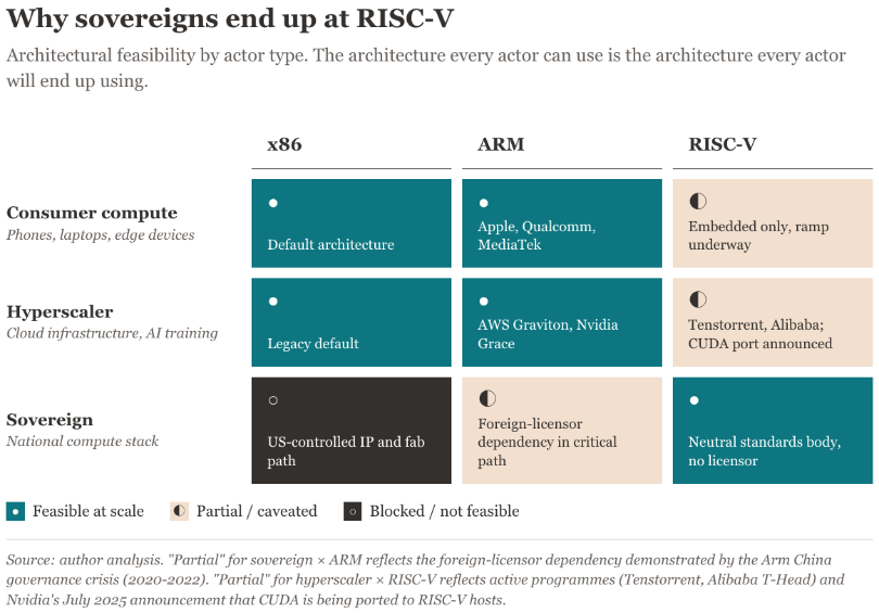
The European case is documented through SiPearl and the European Processor Initiative (EPI). SiPearl is a French-incorporated chip designer founded inside EPI, capitalised through a series of EuroHPC and France 2030 grants alongside a roughly hundred-and-thirty-million-euro Series A. The Rhea-1 processor taped out in November 2025 and will sample in early 2026 inside JUPITER, Europe’s first exascale supercomputer at Forschungszentrum Jülich. Rhea-2 is scheduled for 2026 in Europe’s second exascale system, the Jules Verne installation in France. The EPI roadmap explicitly includes RISC-V acceleration components, and the EU’s separate DARE programme is funding RISC-V development directly. The trajectory is the same as everywhere else: ARM as the transitional architecture, RISC-V as the destination.
The Chinese case is further along on RISC-V deployment than is generally recognised in the Western press. T-Head, the Alibaba semiconductor subsidiary, has shipped over four billion XuanTie cores cumulatively across its embedded and application-processor lines, with the open-source variants on GitHub since 2021. The server-grade XuanTie C930 launched in February 2025; the C950 entered production in early 2026 with reported initial deliveries of 470,000 units and a ¥10bn annualised run rate.
4bn+
Cumulative XuanTie RISC-V cores shipped by Alibaba’s T-Head — the clearest sign China’s sovereign-compute bet has already moved from roadmap to volume production.
The Indian case is the cleanest documentation of the policy choice, and also the earliest-stage. The India Semiconductor Mission 1.0, approved December 2021 with a seventy-six-thousand-crore (roughly ten billion dollar) incentive framework, has approved ten projects across six states with total investment commitments of around nineteen billion dollars by end-2025. The Digital India RISC-V Programme, run under the Ministry of Electronics and Information Technology, funds an indigenous-processor portfolio of half a dozen named families, all RISC-V, all explicitly framed in Indian government communications as eliminating “license costs” and supporting “digital sovereignty.” India does not yet have a comparable operational deliverable to Europe’s JUPITER tape-out or China’s XuanTie production volumes, but the policy commitment is the most explicit on the record. The phrase “digital sovereignty” is not a Western analyst’s translation; it appears in the Indian government’s own press releases.
A caveat on timeline is in order. RISC-V has the architectural neutrality the structural argument requires; it does not yet have ARM’s software ecosystem maturity. ARM took roughly a decade after Graviton 1 to reach credible parity with x86 on enterprise software porting; RISC-V is several years behind ARM at the equivalent stage. Sovereign-compute mandates can fund hardware substantially faster than they can fund the toolchain, application porting, and operator know-how that hardware adoption requires. The trajectory is set; the calendar is not.
Three independent blocs, three independent capital structures, three independent forcing functions, the same architectural answer. The convergence described in section 4 between Apple, AWS and Nvidia repeats here between the EU, China, and India. The mechanism is the same — every dependency layer in the compute stack is being addressed by the actors with the resources and the motivation to address it — and the answer is the same: open IP at the architectural layer, with the fab layer following on its own timeline.
What is up for scraps is every part of the existing compute stack that depends on an externally-controlled licensor in the critical path: the cost structure of the budget Windows laptop, eaten by yield-tail silicon Apple did not have to design; the margin pool of the x86 server market, eaten by Graviton and Grace; the Arm Ltd royalty layer, eaten by the same logic that is eating x86 applied one stack-level up; and the geographic concentration of advanced-node fabrication, eaten — slowly, against fierce resistance, but visibly — by domestic equipment programmes in the blocs that cannot afford the dependency.
What remains is the silicon itself.
7. What’s left
x86 did not lose to a better architecture. It lost because the world stopped being able to afford the dependencies that came with it, and because the volume flywheel had already made ARM cheaper even before the political question became acute. By the time the conclusion arrives at retail, in the form of a $599 laptop selling out for April, the work is mostly already done.
The MacBook Neo is the visible end of a structural shift that has been running underneath the industry for a decade. Every major actor with the resources to make a silicon-architecture decision — Apple, AWS, Nvidia, the European Union, India, China — has independently arrived at the same architectural answer through completely different forcing functions. Whether cost, workload fit or geopolitics: the destination is the same. That is not a passing fashion, it is a structural outcome.
The incumbents will be last. Not because they are blind, but because the institutional cost of seeing it clearly is, at every decision point, higher than the cost of not seeing it. Their customers want compatibility. Their margins fund the engineering programmes that any pivot would require. Their public communication strategy cannot say what their roadmap engineers know. The trap is not stupidity. The trap is incentive structure.
The Internet’s architectural history is instructive here. TCP/IP outlasted every proprietary networking stack precisely because it was unowned: in a world of competing blocs, the standards that survive are the ones nobody can block. ARM itself is not the end of the road: the royalty layer that ARM Ltd represents is the same class of dependency that made x86 politically untenable, one abstraction level up. The architecture most likely to win the cycle after this one is the one whose IP belongs to everyone. The EU is funding it. India is funding it. China is shipping four billion units of it. The cycle is already in motion.
There are a few ways this could fail. Intel succeeding as a merchant foundry on advanced nodes would let it monetise every architectural transition rather than fighting one. ARM consolidating its licensee base and using Armv9 royalty rates aggressively could capture more of the value the structural argument routes to open IP. A material thaw in the US-China relationship would reduce the urgency of sovereign-compute investment. And the software-ecosystem chasm between RISC-V and the production toolchains could persist longer than hardware programmes anticipate. Each is plausible. None of them resolves the structural argument; they only change the slope of the curve.
The MacBook Neo, then, is the visible part of a much larger sorting. What gets left for scraps is every part of the existing compute stack that depends on an externally-controlled licensor in the critical path: Intel and AMD’s x86 server and laptop margin pools, Qualcomm’s Windows-on-ARM platform play, the Arm Ltd royalty layer one stack-level up, and the geographic concentration of advanced-node fabrication that has anchored the West’s compute leverage for thirty years. Everything except the architecture nobody owns.
The last instruction set will be the one nobody owns.