1. The wafer that does not exist
On 23 April 2026, SK Hynix — a Korean memory manufacturer that is neither the largest semiconductor company in the world nor the most strategically positioned in the AI value chain — reported a first-quarter operating margin of 72 per cent. The figure surpasses TSMC’s same-quarter 58.1 per cent. It surpasses Nvidia’s most recently reported operating margin (Q4 calendar 2025; Nvidia’s calendar Q1 reports late May), and the latest reported margins of every other publicly traded technology manufacturer of comparable scale, including Apple and Microsoft. Hynix sells DRAM. DRAM has been treated as a commodity for thirty years.
The 72 per cent is not a single-company anomaly. Micron, the only American manufacturer in the segment, posted a 67 per cent GAAP operating margin for its quarter ending in February — its highest in the company’s history, and a 45-percentage-point increase from a year earlier. Samsung’s Device Solutions division, which houses the company’s memory operations, posted Q4 2025 operating profit of ₩16.4 trillion on ₩44 trillion of revenue; Samsung does not break out memory operating profit at the segment level, but Korean securities analysts estimated DRAM operating margin above fifty per cent and ramping. How three independently operated companies in three different countries — with different boards, different cost structures, different capex profiles, different exposure to the AI build-out — came to print the same anomaly across a single earnings season is the question this piece tries to answer.
To begin, look at a fab floor in Korea. Somewhere on the floor there is a wafer. The wafer is real. It has been pulled from a silicon ingot at Shin-Etsu or SUMCO, sliced into a 300-millimetre disc, polished to atomic flatness, shipped in a sealed cassette, and stored in the raw-materials inventory of a Samsung or Hynix fab. According to the books, it has been committed to a customer, priced, announced in quarterly earnings, written into revenue models. What has not happened — what is in no rush to happen — is the wafer entering the fab line. It has not been started.
Whether it ever gets started — and whether it becomes a memory chip, and what kind of memory chip — is a decision the manufacturer has not yet made. The same wafer can become any of half a dozen products. Computer memory is not one thing: it is a family of devices that store bits across the modern technology stack, from DDR5 modules in servers and LPDDR5X in smartphones to the high-bandwidth memory stacks bonded to AI accelerators and the small DRAM dies inside routers, thermostats and car dashboards. Until late in the production process, a single wafer is fungible across most of these end products. After that point, it is not.
In October 2025, OpenAI signed Letters of Intent with Samsung and Hynix on the same day for the supply of up to 900,000 DRAM wafers per month for its Stargate data-centre programme. Industry analyst estimates put global DRAM wafer-start capacity at roughly 2.2 to 2.3 million per month for 2025; 900,000 represents around 40 per cent of that base if literally drawn down. “Up to” is the load-bearing phrase: the figure is a ceiling, not a floor, and the actual draw is set by manufacturer execution and buyer take-up. The deal is structured as undiced wafers, with dicing, sorting and packaging left to the manufacturer’s discretion. The contract specifies the wafer. It does not specify what the wafer becomes.
Within weeks, every other hyperscaler followed. Microsoft, Google, Amazon Web Services and Meta sent procurement teams to Seoul. By the end of January, Samsung, Hynix and Micron had each announced that their entire 2026 production — DRAM, NAND, and HBM — was sold out. Three companies accounting for roughly ninety-five per cent of global DRAM supply had committed forward production for the calendar year before it had begun.
The path to those margins is visible in the Q4 2025 reporting. Samsung Electronics’ corporate operating profit of ₩20.1 trillion was up 208 per cent year-on-year — its highest quarterly profit on record, with nearly the entire gain coming out of memory. SK Hynix reported full-year 2025 operating profit of ₩47.2 trillion against TSMC’s same-period 54.0 per cent margin — the first time in seven years that memory profitability had overtaken foundry, with Hynix’s DRAM revenue up 70.6 per cent year-on-year and NAND up 59 per cent. Micron’s first-quarter fiscal 2026 revenue was $13.6 billion, up 57 per cent year-on-year, with DRAM revenue up 69 per cent, NAND up 22 per cent, and Q2 guidance pointing toward $18.7 billion. The trajectory was already steep when Q4 closed; the April 2026 print from Hynix bent it further.
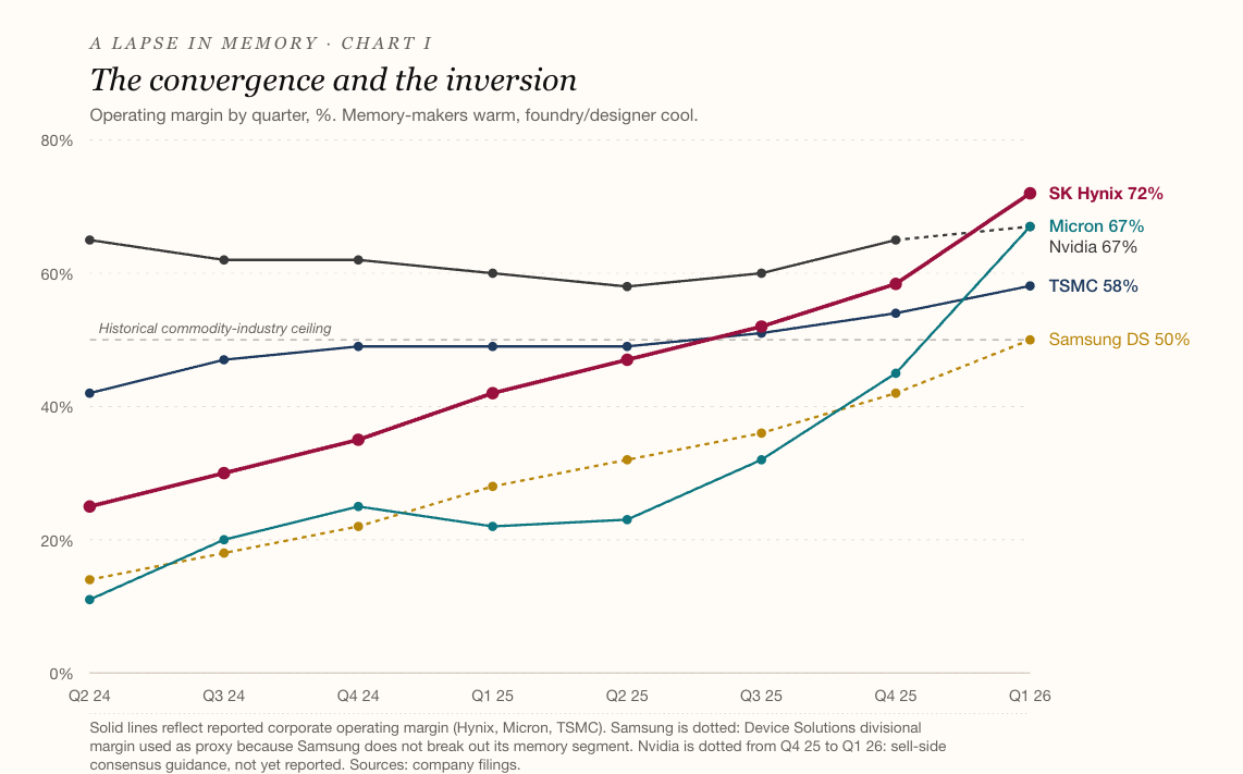
These are not the numbers of a recovering commodity industry. They are the numbers of a strategic asset.
And yet bit shipments — the count of memory cells actually delivered to customers — barely grew. Hynix’s DRAM bit shipments grew low single-digit per cent quarter-on-quarter in Q4 2025; ASP rose mid-twenties. Samsung’s bit growth tracked similarly. Micron’s grew in line with capacity. Across the industry, total DRAM revenue rose 29.4 per cent quarter-on-quarter in Q4 2025 on shipments that, in volume terms, were essentially flat. NAND told a similar story, with manufacturers describing “production restraint” in earnings calls and inventory levels at four to five weeks — near the lower bound of what the industry considers healthy.
Customers are receiving roughly the same volume of memory bits at much higher prices, while Samsung, Hynix and Micron post records and the market wonders where the silicon goes.
72%
SK Hynix’s Q1 2026 operating margin on DRAM — a commodity product — surpassing TSMC, Nvidia, Apple and every other technology manufacturer of comparable scale.
2. From sand to socket
The chain begins with single-crystal silicon ingots, drawn from molten silicon by the Czochralski process, sliced into 300-millimetre wafers and polished to atomic flatness. Five companies globally dominate this stage; two Japanese names, Shin-Etsu and SUMCO, account for roughly half. The wafer then enters a chemistry layer — photoresists, polishing slurries, specialty gases — supplied by a handful of mostly Japanese firms. Helium, used in plasma etch and EUV cooling, is sourced from an equally short list — Qatar, Algeria, Russia, the United States — with Korea, where Samsung and Hynix produce, drawing nearly two-thirds of its helium from a single Qatari hub.
Lithography projects circuit patterns onto the wafer. For the most advanced nodes, this means extreme ultraviolet, and EUV means ASML; the Dutch company is the only producer on the planet. Each EUV machine costs $200 to $400 million and takes eighteen months or more to deliver. SK Hynix recently placed a record $8 billion ASML order. There is no second source.
The fab proper performs hundreds of process steps over several weeks. Four companies — Applied Materials, Lam Research, Tokyo Electron, KLA — supply the bulk of the equipment. For DRAM, Samsung, Hynix and Micron account for ninety-five per cent of global output. NAND adds Japan’s Kioxia and SK Hynix’s Solidigm subsidiary; the top three still control most of the market. Crucially, DRAM and NAND share most of their upstream chain — the same polysilicon, photoresists, lithography slots, helium and specialty gases. A 1c-node DRAM line and a 321-layer NAND line look different inside but compete for the same EUV deliveries and the same fab construction queues.
What emerges from the fab is a patterned wafer.
A patterned commodity DRAM wafer is fungible — to a point. The same wafer, processed on the same line, can be diced and packaged as DDR5 server memory, as LPDDR5X for a smartphone, or as GDDR7 for a graphics card, depending on how its dies sort and bin. NAND has narrower fungibility but the same logic within a given product family. The decision is not made in the fab. It is made at dicing — and once dicing happens, the optionality closes. The HBM packaging line cannot be redirected to produce DDR5 modules; a die diced as commodity DRAM cannot be unpackaged and stacked into HBM. Up to dicing, a wafer is an option. After dicing, it is a product.
Dicing is also where binning happens for most commodity products. Each die is tested at speed, voltage and yield. Strong dies become premium product; weaker dies are sorted into lower bins, with the worst becoming embedded memory for routers, thermostats and car dashboards. The bin cascade is the industry’s standard release valve. HBM is the salient exception: an HBM-bound wafer is committed to HBM during front-end processing, drilled with through-silicon vias, thinned, and given HBM-specific I/O — modifications that cannot be undone. By dicing, the dies are HBM-specific. A die that fails HBM specification cannot be sold as a slow DDR5 chip or relegated to embedded use. It is scrap.
The OpenAI Letter of Intent reserves wafers, not products. The contractual instrument captures the silicon at the point in the chain where optionality is highest, and leaves the back-end decisions in the hands of the manufacturer. Three companies — Samsung, Hynix, Micron — sit at the only stage that decides whether the silicon becomes a server DIMM, a smartphone module, an SSD, a graphics card, or the memory backbone of an AI accelerator. They are not the only chokepoint in computer systems; they are the chokepoint that has chosen to use its leverage.
3. The disconnect
Revenue records produced by selling roughly the same number of bits at much higher prices is the kind of result that, in a normal commodity industry, prompts a question. Either the demand side has run far ahead of the supply side and the manufacturers are catching up — in which case bit shipments would be growing alongside prices, with utilisation pushed to the limit — or something else is going on.
Bit shipments are the cleanest available measure of physical output. A bit is one stored zero or one; bit-shipment growth strips out price effects and product-mix shifts and asks the simple physical question of how much memory the industry actually delivered. Across calendar 2025 the answer was healthy — DRAM bit demand grew in the low twenties, NAND in the high teens. But the growth was front-loaded. By the fourth quarter, with prices rising fastest, physical output was barely moving. SK Hynix’s DRAM bit shipments grew only a low single digit percentage quarter-on-quarter while ASP rose in the mid-twenties. Industry-wide DRAM revenue rose nearly thirty per cent over the same quarter on shipment volumes that were essentially flat.
The price increase is doing the work. A standard DDR4 chip that traded around $1.30 at the start of 2025 sold above nine dollars by year-end. Server DRAM contracts for Q1 2026 were pitched 60 to 70 per cent above the prior quarter, with another roughly 30 per cent uplift queued for Q2. Cumulative server contract pricing is on track to nearly double across mid-2025 to mid-2026, with manufacturers pre-warning of further stepwise increases through 2027.
Ordinarily, a price spike of this magnitude prompts a supply response. Fabs run hotter. Capacity is brought online faster. Lines scheduled for retirement are kept open. None of these things are happening at scale. Samsung, Hynix and Micron all increased capital expenditure for 2026, but the resulting capacity does not arrive in volume before 2027 because the fabs in question are still under construction. The capacity that exists in 2026 is the capacity that existed at the end of 2025, run with what Korean securities analysts politely describe in their notes as “production restraint.”
The structural lever sitting underneath all of this is high-bandwidth memory. HBM is built from DRAM, but it is not commodity DRAM — and a wafer redirected from commodity output to HBM removes substantially more than one wafer’s worth of bits from the broader market. Across calendar 2025, the share of DRAM wafer capacity allocated to HBM rose from the low double digits to a band of roughly 18 to 28 per cent depending on the manufacturer. That is a large reallocation in a market that grows by single-digit percentages a year.
This produces a tripartite supplier base running its capacity at levels that maximise margin rather than volume, allocating its best wafers to a captive AI segment, and watching commodity prices rise as a function of the residual scarcity its own allocation choices have produced.
Which leaves a question. The OpenAI Letter of Intent reserved up to 900,000 wafers per month — a figure that, if literally converted to product, would consume roughly forty per cent of global DRAM capacity. Either it is a maximum that will not be approached in practice, or the manufacturers will need to expand capacity to honour it, or the wafers being booked are not all expected to be physically produced.
900,000
Wafers per month OpenAI’s Letters of Intent reserved from Samsung and Hynix — roughly forty per cent of global DRAM wafer-start capacity, if literally drawn down.
The earnings calls, the capex plans, the bit-shipment numbers and the inventory trajectories all point to the third reading. The structurally similar argument has been made about the broader AI-infrastructure build-out — that the announced spending and the announced capacity do not reconcile when measured against power, water and grid-interconnect availability — but the memory case is the cleaner one, because the contractual instrument captures the silicon at exactly the point where physical realisation can be deferred without breach.
4. Phantom capacity
The mechanical case begins with what an HBM stack actually is. HBM is eight to sixteen DRAM dies stacked vertically and packaged as a single module that sits next to a GPU on an AI accelerator board. The dies are committed to HBM at the front end — through-silicon vias drilled, wafer thinned, HBM-specific I/O patterned — modifications that cannot be undone. HBM4 also requires the latest photolithography, with yields running far lower than mature commodity DRAM during ramp. Combine the wafer-area overhead from TSV structures, the front-end yield haircut, and the closed bin cascade, and the result is what Micron has acknowledged on its earnings calls: every wafer redirected from commodity DRAM to HBM removes roughly three wafers’ worth of usable commodity bits from the broader market.
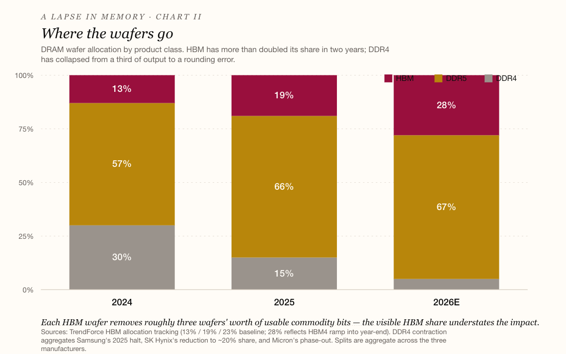
The mix shift is, on its face, a product strategy. HBM is more profitable per wafer than commodity DRAM, and a profit-maximising manufacturer allocates constrained capacity to the highest-margin product. Each of the three is doing exactly this in its own interest. With three suppliers facing the same incentives, the displaced commodity demand has nowhere to go.
This brings us back to the wafer that does not exist. The OpenAI Letter of Intent reserves wafers as undiced silicon: dicing, binning, packaging and the choice between commodity DDR5 and HBM are all manufacturer decisions made after the wafer is produced.
There are three physical possibilities for the manufacturer holding such a contract. Each lives upstream of dicing, in the scheduling of fab capacity. First: schedule wafer starts on the HBM track and ship the resulting HBM. The contract is fulfilled. Second: schedule wafer starts on the commodity track but run those lines below maximum utilisation, capturing the spot-price effect on residual commodity supply. Third: don’t schedule the wafer starts at all. The capacity the LOI reserves is fab-time — slots in the wafer-start queue, EUV machine-hours, packaging-line allocations. Fab-time that is reserved but not scheduled costs the manufacturer almost nothing to hold; raw 300mm substrate wafers, at roughly two hundred dollars each, sit on the balance sheet as cheap raw-material inventory. The expensive inputs — depreciation, chemicals, helium, labour, EUV hours — are only consumed when a wafer actually enters the line. The wafer the contract specifies is real silicon on a fab shelf. It is unstarted because the manufacturer has chosen not to schedule the fab-time that would turn it into product. Phantom capacity, in this industry, is the unstarted wafer.
A fourth, intuitive possibility — schedule the starts, run the wafers, hold the resulting product unsold in finished-goods inventory — is ruled out by the data. At the end of 2024, the industry held thirteen to seventeen weeks of DRAM finished-goods inventory. By October 2025, that figure had fallen to two to four weeks; NAND ended the year at four to five. Inventory is being consumed, not built. The product that does get manufactured is leaving the warehouses. It is just not being manufactured in volumes commensurate with the prices being charged.
That leaves the first three, and the earnings-call language confirms a mix of all of them is in operation. Hynix’s commodity DRAM bit shipments grew low single-digit per cent quarter-on-quarter in Q4 2025 against an ASP rise in the mid-twenties — the gap is the second option, with the third reinforcing it. Samsung’s substantial allocation of Pyeongtaek capacity to HBM4 base-die production for 2026 is the signature of the first. Samsung Securities described the situation to investors in February as “production restraint” — the polite term, used in earnings notes, for capacity that exists and is not running flat out. The disaggregation between mechanisms is not publicly disclosed, but the weights can be triangulated: HBM allocation in the high teens to high twenties of DRAM capacity at a 3:1 displacement ratio against bit-shipment growth in the low single digits implies the diversion mechanism dominates, with under-run and unstarted wafers accounting for the residual.
There is an alternative reading of the same data — that manufacturers are running flat-out and simply cannot produce more because HBM4 yields are difficult, the 1c node ramp has yield haircuts, and TSV stacking imposes its own losses. If that were the binding constraint, output would fall while unit costs rose; margins would compress, not expand. The Q4 2025 and Q1 2026 numbers run the opposite way. Yield-limited production produces compressing margins on rising costs; the recent prints describe expanding margins on rising prices, which is the profile of restraint, not technical failure. Yield is real but it operates through the architecture rather than against it: a manufacturer ramping HBM4 yields from forty to seventy per cent over several quarters can have expanding margins and genuine supply constraints simultaneously, and the architecture is consistent with that.
This is what an option held against both sides of the market looks like — except the buyer is holding one too. AI capacity at scale is constrained not by chips but by the operational infrastructure to run them: substations, switchgear, water rights, fibre, cooling, staffing, grid interconnect. Call these warm sockets: the operating data-centre footprint that has to exist before a single accelerator can be put under load. The chip-side Letter of Intent is therefore not a procurement document but an option contract on warm-socket build-out. Every wafer reserved-but-not-drawn is a wafer the buyer has not had to find power, racks or operators for, and a wafer no competitor can buy. The reservation is itself the moat.
The market state is therefore not three manufacturers extracting rent from a captive hyperscaler. It is two sides of a market quietly aligned on a shared incentive: minimise physical realisation. The manufacturer prefers the unstarted wafer — fab-time costs almost nothing to hold and the capacity cannot be redirected to anyone else. The hyperscaler prefers the unstarted wafer — every undrawn wafer is a warm-socket commitment not yet made and a wafer no competitor can access. Whether prepayment, reservation fees or pure queue-position commitments back the LOI, the practical effect is the same: capacity sits booked but unstarted, with optionality preserved on both sides. The commodity customer pays for the residual scarcity. The market state extracts rent from outside the closed circle and distributes the gains within it.
5. The historical rhyme
What locks this market state into place is the contractual architecture surrounding it. Through Q4 2025 and Q1 2026, Samsung and Hynix explicitly refused the multi-year long-term agreements their buyers were requesting, requiring quarterly contracts with stepwise price increases. Microsoft, Google and Amazon Web Services received the same terms as everyone else. Korean financial press reported that the manufacturers were anticipating stepwise DRAM price increases each quarter through 2027 and were not interested in agreements that would prevent them.
Then, in March and April 2026, the position reversed. Micron disclosed its first five-year Strategic Customer Agreement on its Q2 fiscal 2026 earnings call. Samsung opened negotiations with Google and Microsoft on three-to-five-year deals reportedly worth over $10 billion in total, with prepayments of ten to thirty per cent. Hynix entered final coordination with Microsoft on multi-year DDR5 supply with minimum price floors and prepayment terms. When buyers wanted security at peak prices, manufacturers refused; when manufacturers wanted to cement peak prices into multi-year contracted revenue, they offered the same buyers the structure they had previously refused — at peak prices, with prepayment. The contracts are not symmetric. They were not designed to be.
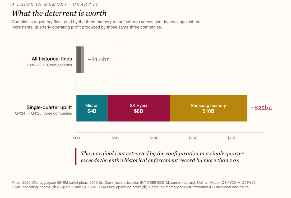
This is the second time the same three companies have produced this outcome. Samsung, Hynix and Micron have been here before, through five credible rounds of cartel accusations, prosecutions or class actions over the past two decades: the 2005 US DOJ investigation that produced guilty pleas and $646 million in fines, with five executives serving a combined 3,185 days in federal prison; the 2010 European Commission case adding €331 million; a 2018 class action in California; a parallel Chinese antitrust raid the same year; and a second class action filed in 2021. Prices rise sharply across all three suppliers in apparent lockstep. Defendants describe their behaviour as rational responses to market conditions. Increasingly, the courts agree.
In March 2022, the US Court of Appeals for the Ninth Circuit issued a published opinion affirming dismissal of the second indirect-purchaser class action — In re DRAM Indirect Purchaser Antitrust Litigation, No. 21-15125 — binding precedent in the Ninth Circuit and influential nationally. The court applied the Twombly pleading standard, under which a Sherman Act conspiracy claim must push from “conceivable to plausible.” Crucially, this was a Rule 12(b)(6) dismissal: the court tested the complaint at its most favourable, assuming every factual allegation was true, and still held that the plaintiffs had not stated a claim. The manufacturers’ contemporaneous capex cuts, public statements about capital discipline and supply restraint were “more suggestive of lawful conscious parallelism than conspiracy” — even with the prior 2005 criminal convictions weighing in plaintiffs’ favour as a plus factor. The ruling did not find the manufacturers innocent. It held that the law, as currently interpreted, cannot reach the conduct without direct evidence of agreement. That is the legal architecture this piece has been describing: oligopolistic interdependence in a concentrated market, not covert agreement, is the protected category.
$22bn
Combined growth in quarterly operating profit across Samsung, SK Hynix and Micron memory divisions between Q4 2024 and Q4 2025 — more than twenty times the entire historical cartel-fine record.
The current market state produces no smoking guns. It does not need them. The capacity allocation decisions are disclosed in earnings calls, the HBM ramp commitments in press releases. The Letters of Intent are public; the multi-year Strategic Customer Agreements are footnoted in 10-Q filings. The legacy node phase-outs are signposted to customers. The Crucial brand exit was a Micron press release on 3 December 2025. Each move, on its own, stands as a defensible commercial decision by a single company. Samsung allocates Pyeongtaek capacity to HBM4 because HBM4 is more profitable per wafer. Hynix runs commodity lines below maximum utilisation because spot prices are extreme. Micron exits Crucial because consumer retail is a low-margin segment and enterprise demand is unmet. None of these decisions requires coordination.
The manufacturers have, on the public record, named what they are doing — but only partially. On a December 2025 investor call, Samsung said it would “minimize the risk of oversupply through a capital expenditure strategy that balances customer demand and pricing.” SK Group’s chairman has publicly forecast that the shortage will last until 2030. The articulated defence is against capex — what they will and will not build — invoking the 2018–2019 collapse, when memory margins fell from above fifty per cent to single digits within four quarters, as the lesson informing 2026 caution. The Twombly shield is strong against parallel capex restraint; each company has independently rational reasons not to build. What the manufacturers have not publicly defended is the operational choice to run existing fabs below maximum utilisation while spot prices are at multi-decade highs. That decision sits in a different doctrinal posture, and no public articulation has been offered for it.
The aggregate is the supply discipline that the 2005 DOJ pleas described. The architecture is what the 2022 affirmance protects. The same companies, having paid fines and served prison time for explicit coordination during 1998–2002, have over twenty years reorganised public conduct, capital allocation and product portfolios around the doctrinal gap that lawful conscious parallelism creates. This is not concealed crime. It is settled-doctrine compliance, in a market structure where the doctrine permits oligopolistic interdependence to produce cartel-equivalent outcomes.
Cumulative historical fines for explicit cartel conduct — the 2005 DOJ pleas plus the 2010 EU action — come to roughly a billion dollars in current-dollar terms. Compare this to the incremental profit the current arrangement has produced, not to total memory profits, much of which would exist under any reasonable market structure. Across the three companies, single-quarter operating profit between Q4 2024 and Q4 2025 grew by roughly $22 billion: Samsung memory by an estimated $10 billion, SK Hynix by $8 billion, Micron by $4 billion. The marginal rent extracted by the market state, in a single quarter, exceeds the entire historical enforcement record by more than twenty times. Even if regulators successfully prosecuted the present arrangement under some future law, the arithmetic of deterrence has broken down. Any future fines would be absorbed as a cost of doing business line item.
6. The empty fab and the burning flare
A modern memory fab is a ~$15 billion building containing several hundred pieces of single-purpose equipment, much of it on multi-month delivery schedules and several years of waiting list. Its fixed costs — depreciation, real estate, building services, the salaries of thousands of skilled employees — accrue regardless of whether wafers are being processed. Variable costs scale with throughput: chemicals, gases, EUV machine-hours, labour to operate and inspect, yield-loss equipment depreciation. Every fab has an optimum operating point at which unit cost is minimised: below the engineering maximum, but well above idle. Running it well below that optimum is a deliberate choice. In a competitive market, the textbook response to spot prices several multiples above marginal cost is to operate above optimum, not below: each additional wafer captured at the spot premium more than covers the rising marginal cost. The three are doing the opposite.
Hynix’s Q4 2025 — low single-digit bit growth against a mid-twenties ASP rise — was not a sudden equipment failure or a yield collapse. It was a deliberate decision to start fewer wafers than the lines could absorb at optimum utilisation. Samsung’s “production restraint” language was a description of a chosen operating posture, not a description of constraint imposed from outside. Across the industry, fabs that are nominally “sold out for 2026” are running at less than the throughput their construction specifications could support. The capacity exists as physical infrastructure. The capacity exists as forward financial commitment. The capacity does not exist as actual silicon being moved through process steps at the rate the fab was sized for.
Ras Laffan, the world’s largest single LNG production hub, came under Iranian drone attack in early March 2026. QatarEnergy declared force majeure on deliveries from the complex on 4 March; the Strait of Hormuz closed to Western commercial shipping in the same week. Repair timelines were estimated at three to five years.
Aside from LNG, Ras Laffan also produced helium as a byproduct, sharing the same wells and separation infrastructure. Qatar accounts for roughly thirty to thirty-four per cent of global helium production, and South Korea sourced 64.7 per cent of its helium imports from Qatar in 2025, making Samsung and Hynix the most exposed memory manufacturers in the world to a Ras Laffan event. Spot helium prices rose more than 40 per cent within weeks. Airgas, the largest US distributor, declared force majeure on US deliveries on 17 March. Helium consumption per wafer rises as nodes shrink, particularly for the EUV-intensive processes used in Hynix’s 1c DRAM and Samsung’s HBM4 base-die production.
None of this caused the supply discipline. It was in place by late 2024, before Ras Laffan was a known risk and before the Stargate Letters of Intent were signed. What the strike changed was not the stance but its public defensibility. A fab running at reduced utilisation because the manufacturer has chosen to constrain supply looks identical, from the outside, to a fab running at reduced utilisation because it cannot get enough helium for its EUV tools.
The Korean Fair Trade Commission’s pricing investigation, opened in early 2026, now faces an evidentiary problem its 2018-vintage equivalents did not: the manufacturers can point to a documented force majeure on a critical input, originating in a war on the other side of the world, as the reason their commodity output has fallen short. The stance was already in place. Ras Laffan made it speakable.
7. The release valves that aren’t releasing
Memory cycles end. Prior squeezes — 2017–2018, 2013, the 2007 spike that brought the cartel period to a close — all eventually broke when supply caught up with demand. The dominant historical mechanism was generational divestment. Each major node transition — SDRAM through five generations of DDR, plus the GDDR fork for graphics — made the previous generation’s leading-edge fabs structurally obsolete for the manufacturer’s roadmap. The leading edge moved on; the older fab became dead capital unless its capacity was redeployed. Selling, transferring or winding down those fabs into second-tier hands made commercial sense and produced second-source supply for the channel. China’s CXMT, Taiwan’s Nanya and smaller players in Japan and Korea each absorbed depreciated equipment from prior handoffs and produced second-source DRAM that disciplined spot pricing on commodity bits. The architecture by which leading-edge profitability was extracted while the rest of the channel was supplied at competitive prices was a function of this divestment cascade.
The current cycle is different. The leading edge is not the next DRAM generation — it is HBM, a different product class layered on top of DRAM rather than replacing it. A leading-edge HBM line and a current-generation commodity DDR5 line do not displace each other. Both are profitable, both are wanted by different customers, and the manufacturer has no incentive to retire either. The previous generation is no longer dead capital; it is current capital. The mechanism that historically forced divestment has been disrupted by the geometry of the technology shift itself.
Hynix’s older Wuxi fab, historically a candidate for handoff, was instead upgraded from the 1z to the 1a node during 2024–2025. Samsung has done similar at Pyeongtaek. The DDR4 end-of-life that Samsung and Micron announced was reversed in mid 2025 when DDR4 spot prices inverted above DDR5: rather than exiting, Samsung signed long-term, non-cancellable contracts with named server clients in Q1 2026, earmarking revived DDR4 supply for hyperscaler and enterprise buyers rather than the channel. NAND tells the same story. Samsung is ending MLC NAND production in 2025; Kioxia is phasing out 2D flash and early-generation BiCS3 by end of 2028; the older capacity is being retired internally rather than redirected to secondary suppliers.
CXMT’s market share has grown from 3 to 5 per cent over the past year. Whatever role it eventually plays in supply normalisation, it cannot replace the divestment cascade — partly because US export controls have constrained its access to advanced lithography tools, partly because its capex is absorbed by upgrading from DDR4 to DDR5 under direction from the Chinese government. The trickle-down of used equipment from Samsung, Hynix and Micron retirements to second-tier fabs has been redirected: the same equipment is being refurbished into the manufacturer’s own greenfield projects in Texas, Idaho, New York, Singapore and Pyeongtaek under CHIPS Act and equivalent funding.
The downstream channel exit is the most visible consequence. On 3 December 2025, Micron announced it was winding down its Crucial consumer brand — twenty-nine years old, founded 1996 — with last shipments scheduled for February 2026. Sumit Sadana, Micron’s chief business officer, explained the decision in plain English: “improve supply and support for our larger, strategic customers in faster-growing segments.” The DIY builder, the small system integrator, the upgrade buyer: all are now serviced only by aftermarket brands like Corsair, Kingston and G.Skill, who buy their dies from Samsung and Hynix at whatever the seller’s-market quarterly contract permits.
Each closure is independently defensible. Hynix’s Wuxi upgrade is a competitive response to CXMT’s DDR5 ramp. Samsung’s DDR4 reversal is a margin opportunity. Micron’s Crucial exit is a portfolio decision. The channels through which prior memory squeezes ended have, for this cycle, been closed.
8. The downstream tax
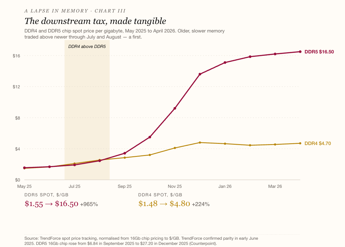
With the release valves closed and the setup legitimised, the question becomes who pays. Contract DRAM pricing is private. The retail aftermarket channel is the only public longitudinal price series for memory and is the lead indicator the rest of the chain catches up to. Between May and December 2025, on the retail price tracker PCPartPicker, the average price of a 32GB DDR5-6000 memory kit rose from approximately $120 to $410 — a 242 per cent increase in seven months. A 64GB kit went from $210 to $750. The Crucial Pro DDR5-6000 32GB kit that Micron itself had been selling at $80–100 throughout 2024 and into mid-2025 traded above $360 by January 2026. At the chip spot level, the inversion was sharper still: TrendForce confirmed that DDR4 and DDR5 chips reached price parity in early June 2025, with DDR4 trading above DDR5 through July and August. Older, slower, cheaper-to-make memory commanding a premium per gigabyte over newer, faster product was unprecedented in DRAM’s history. In Q4 as DDR5 chip prices rose 298 per cent between September and December, leaving both at structurally elevated levels.
The signs of stress accumulated quickly. An enthusiast gamer 64GB DDR5 kit by late November 2025 retailed above the launch price of a PlayStation 5 Pro. A Texas Micro Center store removed posted DDR5 prices and instructed customers to ask staff. Motherboard sales fell 40 to 50 per cent year-on-year as builders cancelled or deferred upgrades. CyberPowerPC, the prebuilt-PC system integrator, announced on 25 November 2025 that its DRAM input costs had surged 500 per cent since October — and raised system prices effective 7 December.
The forward forecasts have been playing catch-up to the retail data. Gartner in February 2026 projected a 130 per cent memory price surge by year-end, with PC ASPs rising 17 per cent and smartphone ASPs 13 per cent; and forecast that the sub-$500 PC segment would disappear by 2028. PC lifetimes were forecast to rise 15 per cent for business buyers and 20 per cent for consumers. IDC’s forecast for global PC unit shipments in 2026 stands at minus 11.3 per cent. These are contract-price projections; the retail market has already overshot them.
Vendor responses follow a predictable shape: front-loaded inventory in Q4 2025, then spec downgrades through 2026 — 12GB to 8GB at the mid-range, 8GB to 4GB at the low end, smaller storage at the same price points. Apple and Samsung are structurally hedged via long-term agreements signed earlier; mid-tier and budget OEMs absorb the squeeze on thinner margins. Samsung’s own Galaxy S26 is expected to launch with a 16 per cent LPDDR5 cost increase, despite Samsung being its own supplier. Samsung Semiconductor will not commit to bulk-rate supply for Samsung Electronics’ phone division — the wafer goes to whoever pays most.
In the server market, contract DRAM prices for Q1 2026 were pitched 60 to 70 per cent above Q4 2025, with another roughly 30 per cent uplift for Q2. Cumulative server DRAM costs are on track to nearly double across mid-2025 to mid-2026. Hyperscalers either absorb the cost as capex inflation or pass it through to cloud customers. Networking, automotive, industrial and embedded buyers sit third-priority behind hyperscaler-AI and enterprise server.
Hyperscalers and frontier-AI buyers did not acquire pricing power against the rest of the technology supply chain by accident. They built it through the LOI architecture, in commercial alignment with the manufacturers who hold the only relevant capacity. Everyone downstream — from a PC builder in Rotterdam to a router OEM in Shenzhen to a regional hospital procuring industrial PCs — pays a tax that funds both the manufacturer’s supply discipline and the hyperscaler’s competitive moat. The 2025–2026 retail spike is the visible tip of a capital reallocation in which the Big Five hyperscalers’ 2026 capex — projected by CreditSights at around $602 billion, with consensus estimates ranging up to $700 billion as Q4 earnings landed — flows in part through Samsung, Hynix and Micron as committed forward revenue. The European Commission has not yet weighed in, though Article 101 of the TFEU covers “concerted practices” alongside formal agreements — a threshold lower than the post-2022 Sherman Act bar. No public signal has yet emerged from any member-state authority.
9. The lapse
Memory has lapsed from commodity to strategic asset. The manufacturers who produce it have lapsed in the regulatory sense — the supply-disciplined behaviour that DOJ prosecuted in 2005 has been reproduced in 2026 through legitimate, separately-defensible commercial choices that no current law can prosecute. The hyperscalers have not lapsed; they structured the LOIs correctly. That structure gives both sides aligned incentives to minimise actual draw, and the prepayment funds the supply discipline that prices the rest of the world’s alternatives out of the market. Regulators have lapsed in distinguishing this from collusion. Consumers have lapsed in noticing — the price increase reaches them not as a single visible event but as a downgrade, a deferred upgrade, a vanishing budget tier, a four-figure RAM kit they decide not to buy.
The forward question for the next six to twelve months turns on whether the manufacturers print the silicon their LOI counterparties have committed to take. If they do not, meaning warm-socket build-out lags, demand pulls in well below the LOI ceiling. The helium constraint becomes the ratified explanation, the SCAs convert supply tightness into multi-year contracted revenue at peak prices, and the downstream tax hardens through 2026 and into 2027. No party inside the closed circle needs to take any action. If they do, meaning hyperscaler warm-socket build-out catches up with paper LOI capacity, the spot market eases, commodity bit supply expands, the market state relaxes, and Korean memory operating margins compress hard. The manufacturers give up rent they have already booked. The reverse trade in the equity is interesting in that scenario. The default is the first.
Three companies that paid roughly a billion dollars in fines for explicit price-fixing in the past two decades have produced, through years of reorganisation around the legal architecture, a configuration that delivers the same supply-disciplined outcome in 2026 at margins that make those fines a rounding error — and they have done it in commercial alignment with the largest buyers in the market. That alignment is funded, not passive: the prepayments and reservation fees flowing from hyperscaler to manufacturer pay for the supply discipline that turns the rest of the world’s memory demand into a competitive moat. The 2022 Ninth Circuit affirmance that protects the configuration treats the parallel behaviour as conscious parallelism in a concentrated industry: lawful, settled doctrine. Read narrowly, that is correct. Read at scale, with the deterrent math now broken, the release valves closed, and the buyer side aligned with the seller side, it is the legal foundation of an architecture that prices a meaningful slice of global technology demand against a captive AI optionality whose physical realisation remains, weeks before delivery, undecided.
The wafer the piece opened with sits in raw-materials inventory, real silicon, contracted, paid for. It is unstarted. Whether it ever enters the fab line, and what it becomes if it does, is the question that the rest of the technology supply chain is currently paying to keep open. The 72 per cent operating margin is the price of that question remaining unanswered.